ST8500可編動(dòng)力線通信(PLC)調(diào)制解調(diào)器解決方案
- 發(fā)布時(shí)間:2019-12-07
- 發(fā)布者: 管理員
- 來源: 本站
- 閱讀量:398
ST公司的ST8500可編動(dòng)力線通信(PLC)調(diào)制解調(diào)器系統(tǒng)片上系統(tǒng)(SoC),能在頻率高達(dá)500kHz運(yùn)行任一種PLC協(xié)議.器件架構(gòu)設(shè)計(jì)用于CENELEC EN50065, FCC和ARIB兼容的應(yīng)用兵,支持所有主要的PLC標(biāo)準(zhǔn)如ITU G.9904(PRIME),ITU G.9903 (G3-PLC?)以及其它PLC協(xié)議規(guī)范和演進(jìn).器件包括具有自動(dòng)增益控制的PGA和ADC,具有發(fā)送預(yù)驅(qū)動(dòng)器的DAC,數(shù)字發(fā)送電平控制,以及零交叉比較器.高達(dá)500kHz的PLC信號(hào)帶寬. ST8500具有標(biāo)準(zhǔn)32位ARM? Cortex-M4FMCU可編核,用于協(xié)議上層和外設(shè)管理,最大工作頻率200MHz,嵌入用于代碼和數(shù)據(jù)256kB的SRAM,嵌入96kB數(shù)據(jù)SRAM,8kB共享RAM和引導(dǎo)ROM存儲(chǔ)器.外接3.3V用于I/O和模擬電源,2.5V內(nèi)部線性穩(wěn)壓器用于模擬,1.1V外接電源用于數(shù)字,具有正常,慢,打盹和低功耗模式,采用QFN56封裝,工作溫度-40℃ 到 +105℃.主要用于智能計(jì)量,智能電網(wǎng)和物聯(lián)網(wǎng)(IoT),以及CENELEC, FCC與ARIB兼容的應(yīng)用設(shè)計(jì).本文介紹了ST8500主要特性,基本框圖和詳細(xì)架構(gòu)圖,時(shí)鐘樹和電源方案,以及評(píng)估板EVALKITST8500-1主要特性,框圖和電路圖.
Programmable power line communication modem System on Chip evaluation kit The ST8500 is a fully programmable power line communication (PLC) modem System on Chip (SoC), able to run any PLC protocol in the frequency band up to 500 kHz.
The device architecture has been designed to target CENELEC EN50065, FCC and ARIB compliant applications supporting all major PLC protocol standards such as ITU G.9904(PRIME), ITU G.9903 (G3-PLC?) and many other possible PLC protocol specifications andevolutions.
ST8500主要特性:
? Programmable power line communication(PLC) modem System on Chip
? Integrated differential PLC analog front-end
– PGA with automatic gain control and ADC
– DAC with transmission pre-driver
– Digital transmission level control
– Zero crossing comparator
– Up to 500 kHz PLC signal bandwidth
? High performance, fully programmable realtimeengine dedicated to PLC PHY and real -time MAC protocol management (400 MHzmax. frequency)
– Dedicated code and data SRAM memories
? Standard ARM? 32-bit Cortex?-M4F fullyprogrammable core for protocol upper layers
and peripherals management
– 200 MHz maximum frequency
– 256 kB of embedded SRAM for code anddata
– 96 kB of embedded SRAM for data
– 8 kB of embedded shared RAM
– Bootloader ROM memory
– One Time Programmable (OTP) memorywith dedicated areas available for secure
keys and user information storage
– Serial wire and JTAG interfaces
– 24 multiplexed GPIOs
– 4 general purpose timers
– 1 flexible CRC calculation unit
– 2 USART, 1 UART, 3 SPI, 1 I2C
? Cryptographic engine
– AES 128/192/256 engine
– True random number generator
– Pseudo random number generator
? Clock management:
– 25 MHz external crystal for system clock
– Integrated 25 MHz oscillator (XOSC) withfrequency synthesizer (FS) and pre-scaler
units to generate internal clock signals
? Power management
– 3.3 V external supply voltage for I/O andanalog
– 2.5 V internal linear regulator for analog
– 1.1 V external supply voltage for digital
– Normal, Slow, Doze and low power modes
? Available in QFN56 package
? -40℃ to +105℃ temperature range
ST8500應(yīng)用:
? Smart metering, smart grid and Internet ofThings applications
? Suitable for application design compliant withCENELEC, FCC and ARIB regulations
The ST8500 architecture is composed of the following parts:
1. PLC front-end including digital front-end (DFE) and analog front-end (AFE)
2. Real-time engine: the digital core running the lower layers of the PLC protocol stack
and implementing modulation, demodulation and advanced forward error corrections(FEC) algorithms
3. Protocol engine: the digital core running the upper layers of the PLC protocol stack and
managing the interface with external microcontrollers.
4. Peripherals, crypto, debug section
5. Clock and reset section
6. Power management section
圖1.ST8500基本框圖
圖2.ST8500詳細(xì)架構(gòu)圖
圖3.ST8500時(shí)鐘樹圖
圖4.ST8500電源方案圖
評(píng)估板EVALKITST8500-1
The EVALKITST8500-1 is a platform which allows an easy way to evaluate the features andperformance of a power line communication (PLC) node based on the ST8500 modemsystem-on-chip and the STLD1 line driver.
This user manual explains the EVALKITST8500-1 hardware and software installation, and
details the evaluation of the kits.
This user manual does not explain the functionalities of the various PLC protocols running
on the ST8500. Detailed information can be found in the protocol specific documentation,
available within the software packages, separately delivered under the Software license
agreement by contacting your local ST sales office.
Based on the ST8500 power line communication System on Chip, the EVALKITST8500-1 evaluation kit embeds all the functions required for a turnkey power line communication network.
Depending on the PLC protocol targeted, different firmware releases should be loaded on the host Flash memory. Please check software release availability with your local STMicroelectronics sales office.
Intuitive graphical user interface (GUI) for the Windows? environment allows the user to upgrade the firmware release, configure and control the evaluation kit.
圖5.評(píng)估板EVALKITST8500-1外形圖
圖6.評(píng)估板EVALKITST8500-1框圖
圖7.STM32控制板外形圖
圖8.STM32控制板概況圖
圖9.ST8500模塊外形圖
圖10.ST8500模塊概況圖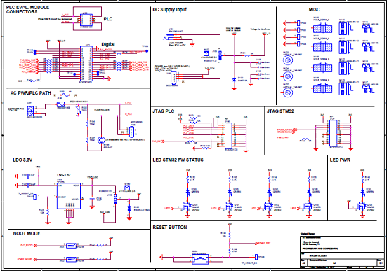
圖11.評(píng)估板EVALKITST8500-1電路圖:EVALST-PLCMB1(1)
圖12.評(píng)估板EVALKITST8500-1電路圖:EVALST-PLCMB1(2)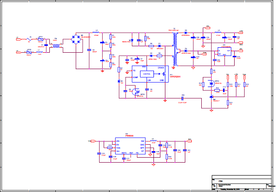
圖13.評(píng)估板EVALKITST8500-1電路圖:PSU_VIPER板
圖14.評(píng)估板EVALKITST8500-1電路圖:ST8500模塊板(1)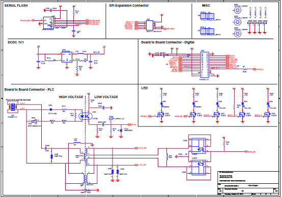
圖15.評(píng)估板EVALKITST8500-1電路圖:ST8500模塊板(2)
詳情請(qǐng)見:
https://www.st.com/content/ccc/resource/technical/document/user_manual/group0/3a/dc/89/3e
/4d/6d/46/d1/DM00467734/files/DM00467734.pdf/jcr:content/translations/en.DM00467734.pdf st8500.pdfen.DM00467734.pdf